
Silvaco FinFet 3d仿真
网上这一部分的资料实在是太少了,只能结合着b站一位同学的专栏和网上的印度老师视频慢慢学习,因为有仿真3D模型的需要,同时学校没有Sentuaraus的License,就只能慢慢学习。
代码:
go devedit simflags="-3d"
#启动devedit,其实应该可以直接使用GUI去进行器件的建模,但是因为教程是在batch mode,也就是输入命令在deckbuild,因此我也现#按照这个来进行仿真学习再说,之后有时间可以去试试看GUI
work.area x1=-0.01 y1=-0.01 x2=0.02 y2=0.045
#定义了你画器件的剖面的区域
region reg=1 mat=Silicon color=0xffccOO pattern=0x4 z1=0.01 z2=0.09
polygon="0,0 0.01,0 0.01,0.015 0,0.015"
#定义1了区域1,也就是silicon的区域,这个区域的截面是用4个点圈起来的,,color是16进制进行表示,在manual中可以看到。#pattern指的是当我们display的mesh黑白的时候的这个黑度,pattern是0-17,但规定不能使用0和17,0是solid,17是empty,意思#就是数字越小越黑
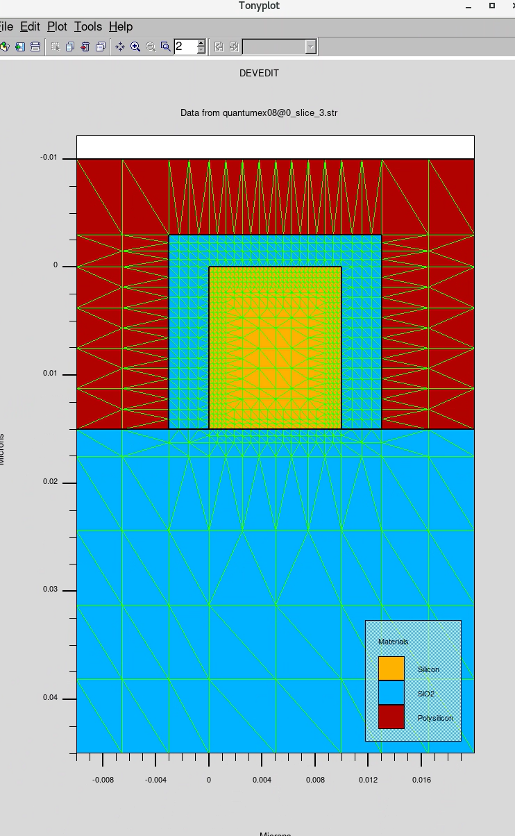
constr.mesh region=1 default max.height=0.01 max.width=0.02
#这里是使用constr.mesh去构建网格,这个之后还是会出现,但是这里是构建整个区域1的网格大小,后面会从中微微调整,就是会在局部让#网格变小,更加精细。default在这里指的是先把这些网格的定义先都重置了。
region reg=2 mat="Silicon Oxide" color=0xff pattern=0x2 z1=0.01 z2=0.09
polygon="0.013,0.015 0.01,0.015 0.01,0 0,0 0,0.015 -0.003,0.015 -0.003,-0.003 0.013,-0.003"
#region2的范围标注,这里是用了很多个点去做,顺逆时针都是可以的
constr.mesh region=2 default max.height=0.001 max.width=0.001
region reg=3 name=gate mat=PolySilicon elec.id=1 work.func=0 color=0xffff00 pattern=0x5 z1=0.035 z2=0.065
polygon="0.013,-0.003 -0.003,-0.003 -0.003,0.015 -0.01,0.015 -0.01,-0.01 0.02,-0.01 0.02,0.015 0.013,0.015"
#在这里是把gate定义成electorde
constr.mesh region=3 default max.height=0.01 max.width=0.02
region reg=4 mat="Silicon Oxide" color=0xff pattern=0x2 z1=0 z2=0.1
polygon="-0.01,0.015 0.02,0.015 0.02,0.045 -0.01,0.045"
constr.mesh region=4 default max.height=0.01 max.width=0.02
region reg=5 name=drain mat=Aluminum elec.id=2 work.func=0 color=0xffc8c8 pattern=0x7 z1=0 z2=0.01
polygon="0,0 0.01,0 0.01,0.015 0,0.015"
constr.mesh region=5 default max.height=0.01 max.width=0.02
region reg=6 name=source mat=Aluminum elec.id=3 work.func=0 color=0xffc8c8 pattern=0x7 z1=0.09 z2=0.1
polygon="0,0 0.01,0 0.01,0.015 0,0.015"
constr.mesh region=6 default max.height=0.01 max.width=0.02
#set meshing parameters
#这里是开始设置一些网格的基本参数吗,我有点不明白为什么不先设置这个。chatgpt说是可以的,我重新跑了也可以的。
base.mesh height=0.01 width=0.005
#设置了mesh的default的参数,这个值是比较小的吗,你可以上面的设置相比看出来。
bound.cond !apply max.slope=28 max.ratio=300 rnd.unit=0.0001 line.straightening=1 align.points when=automatic
#设置网格生成时边界条件的约束,没怎么看懂
imp.refine min.spacing=0.02 z=0
#设置网格的局部细化规则,用于在特定区域(如杂质浓度变化剧烈的区域)生成更密集的网格。min.spacing=0.02:设置网格单元之间的最#小间距为 0.02微米。这意味着在特定区域,网格单元之间的距离不会小于 0.02 微米。z=0:指定网格细化在 z=0 处生效。这可能指的是#器件的某一特定深度层(z轴为0的位置)。
constr.mesh max.angle=90 max.ratio=300 max.height=10000
max.width=10000 min.height=0.0001 min.width=0.0001
#设置网格的全局约束,定义了网格单元的一些参数限制。其实就是没用的,因为最小值太小,最大值太大。
constr.mesh type=Semiconductor default
constr.mesh type=Insulator default
constr.mesh type=Metal default
constr.mesh type=other default
constr.mesh region=1 default max.height=0.01 max.width=0.02
constr.mesh region=2 default max.height=0.001 max.width=0.001
constr.mesh region=3 default max.height=0.01 max.width=0.02
constr.mesh region=4 default max.height=0.01 max.width=0.02
constr.mesh region=5 default max.height=0.01 max.width=0.02
constr.mesh region=6 default max.height=0.01 max.width=0.02
#此命令为绝缘体区域设置默认的网格生成规则,确保绝缘材料区域的网格与其他材料区域的网格划分不同
# Local mesh refinement for specific areas
constr.mesh id=1 x1=0 y1=0 x2=0.01 y2=0.015 default max.height=0.002 max.width=0.002
constr.mesh id=2 x1=0 y1=0 x2=0.001 y2=0.015 default max.height=0.0005 max.width=0.0005
constr.mesh id=3 x1=0.009 y1=0 x2=0.01 y2=0.015 default max.height=0.0005 max.width=0.0005
constr.mesh id=4 x1=0.001 y1=0 x2=0.009 y2=0.001 default max.height=0.0005 max.width=0.0005
constr.mesh id=5 x1=0 y1=0.0145 x2=0.01 y2=0.016 default max.height=0.0008 max.width=0.0008
#这里一开始看可能是觉得是多次一举,其实这里将一些需要精细化网格的区域重新变得更加的小了,可以在之后的图里看出来。
# Now we switch to MeshBuild mode to generate the mesh
MESH Mode=MeshBuild
#只有当 MESH Mode=MeshBuild 被调用时,之前定义的所有网格设置(例如 constr.mesh 中的参数)才会被应用到网格生成过程中。
#仿真器会按照你定义的规则,生成每个区域的网格,并进行必要的细化。
z.plane z=0 spacing=0.1
z.plane z=0.005 spacing=0.1
z.plane z=0.01 spacing=0.1
z.plane z=0.012 spacing=0.1
z.plane z=0.0167 spacing=0.1
z.plane z=0.0233 spacing=0.1
z.plane z=0.0267 spacing=0.1
z.plane z=0.030 spacing=0.1
z.plane z=0.0315 spacing=0.1
z.plane z=0.033 spacing=0.1
z.plane z=0.035 spacing=0.1
z.plane z=0.041 spacing=0.1
z.plane z=0.047 spacing=0.1
z.plane z=0.053 spacing=0.1
z.plane z=0.059 spacing=0.1
z.plane z=0.065 spacing=0.1
z.plane z=0.067 spacing=0.1
z.plane z=0.0685 spacing=0.1
z.plane z=0.070 spacing=0.1
z.plane z=0.0733 spacing=0.1
z.plane z=0.0767 spacing=0.1
z.plane z=0.0833 spacing=0.1
z.plane z=0.088 spacing=0.1
z.plane z=0.090 spacing=0.1
z.plane z=0.095 spacing=0.1
z.plane z=0.100 spacing=0.1
#先生成二维的 x-y 网格,再通过 z 平面的定义扩展成三维网格。
z.plane max.spacing=1000000 max.ratio=1.5
#在这个例子中,max.spacing=1000000 设置了一个非常大的数值,表示相邻 z 平面之间的最大间距可以达到 1,000,000 个单位(通常#是微米,视具体仿真器的单位定义而定)
#max.ratio=1.5 意味着相邻 z 平面之间的网格间距不能超过 1.5 倍。也就是说,如果仿真器在某个位置生成了一个 z 平面,并且它与
#下一个 z 平面之间的间距为 d,那么下一个 z 平面和再下一个 z 平面之间的间距最多可以是 1.5d。
structure outf=quantumex08@0.str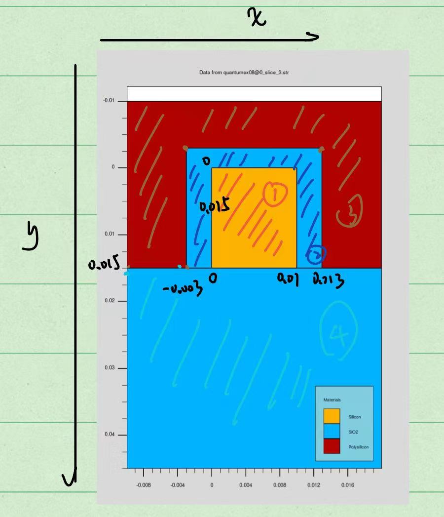
这之后是simulation的部分。
go atlas simflags="-P 64"

#go atlas simflags="-P 64"
#mesh infile=Finfet.str 在这里也可以直接把devedit的mesh结构导入。
set gamma=1.4
set alpha=0.3
#这个set gamma和alpha是为了之后修改参数,就不用去实际的代码里面进行修改了,可以直接在这里进行修改,调参方便。
ELECTRODE name=bulk bottom
#在上面已经定义了drain,source,gate了,所以这里只需要定义bulk,bottom。
#bottom:Places the specified electrode at the bottom of the device and names the
#electrode, substrate.
#意思是给这个点击取名为bulk,然后是在bottom。

DOPING num=1 p.type uniform conc=1e18
#先把整个channel都doping了,然后下面再去重点doping Source和Drain part。
DOPING num=1 gaussian n.type conc=1e21 y.min=0.0 y.max=0.015 z.min=0.010 z.max=0.0233 zlat.char=0.004 char=0.001

DOPING num=1 gaussian n.type conc=1e21 y.min=0.0 y.max=0.015 z.min=0.0767 z.max=0.091 zlat.char=0.004 char=0.001
#这里是在doping source和drain。这里是用了高斯分布。
###为什么没有定义 x?
#这通常意味着掺杂在 x 方向 上是均匀的,即x方向上是均匀分布的。
#lat.char指的就是z的方向的掺杂的范围,特征值越大就代表高斯分布越广。
#小 LAT.CHAR 值:掺杂集中在非常狭窄的区域,导致局部电流较小、开启电压较高,
#适用于某些具有局部化掺杂需求的器件,但可能会导致局部电场过强,影响器件可靠
#性。
#中等 LAT.CHAR 值:带来了较好的均匀性,掺杂分布合理,有较高的电流驱动能力,
#适合大部分器件设计需求。
#大 LAT.CHAR 值:掺杂非常均匀地分布在大面积区域,带来更高的电流驱动能力,但
#可能引发寄生效应,适合需要高驱动电流的应用,但可能影响器件的速度和功耗。

MATERIAL material=Silicon eg300=1.1245 affinity=4.05 permittivity=11.9 ml=0.7 mt1=0.7 mt2=0.7 nc300=2.8e19
#这里是把在devedit上定义的mesh和其他的东西都重新细化的定义,就是定义材料的一些特征。
#eg300 是材料在 300K(室温) 时的 能隙(bandgap energy
#affinity 是 电子亲和势(electron affinity),单位是电子伏特(eV)。
#permittivity 是材料的相对 介电常数(relative permittivity 或 dielectric constant)。
#ml 是材料的 纵向有效质量(longitudinal effective mass)
#mt1 和 mt2 是材料的 横向有效质量(transverse effective mass),也是以电子静止质量为单位的无量纲数值。
#nc300 是材料在 300K(室温) 时的 导带有效态密度(effective density of states in the conduction band)。

MATERIAL material=Oxide eg300=8.05 affinity=1.00 permittivity=3.9 ml=0.3 mt1=0.3 mt2=0.3 nc300=2.8e19 nv300=1.04e19
MATERIAL material=poly eg300=1.1245 affinity=4.05 permitti=11.9

CONTACT name=gate work=4.85
CONTACT name=drain
CONTACT name=source
#这里是定义接触,contact

MODEL fermi bqp.n srh ni.fermi HCTE.EL bqp.ngamma=$gamma bqp.nalpha=$alpha evsatmod=0 fldmob print
#物理模型的調整,主要包含五種類別的方向可以調整,語法最後的print則代表在模擬開始時餵入模型到架構中。
#当使用 print 参数时,ATLAS 仿真器会在终端或日志文件中打印出,目前还是不知道在哪里可以看到。
METHOD maxtrap=6 autonr nblockit=45 bicgst dvlimit=1.0
#这里的maxtrap指的是陷阱态的最大数量。陷阱态是指在半导体器件中由缺陷或杂质引起的能级,这些能级可以捕获或释放电子或空穴,影响器件的电特性。
#FinFET 器件的表面区域较多(例如鳍的侧壁),可能会有更多的界面态或陷阱态影响器件的性能。适当设置 maxtrap 可以帮助准确模拟这些效应,尤其是在高击穿电压或低功耗器件中。
#autonr 是 自动牛顿-拉夫森法(Automatic Newton-Raphson method) 的开关。开启此选项后,ATLAS 会根据仿真过程中遇到的非线性程度,自动调整牛顿-拉夫森的迭代步长。
#nblockit 是 最大块迭代次数。它控制仿真在每个时间步或电压步中,允许的最大块迭代次数
#dvlimit=1.0:限制每次电压步长,确保仿真过程的稳定性,防止电压步长过大导致的收敛问题

SOLVE init

SOLVE vgate=0.2 nocurrent

SOLVE vdrain=0.001 name=drain vstep=0.0005 vfinal=0.01
#为什么1设置vdrain这么小,原因1是这是用在初步仿真,这样子可以更好的收敛;原因2是这是用在低功耗器件上的,所以也不奇怪。
#在低电压下,漏极电流的变化与栅极电压的关系更接近线性,这便于提取器件的导电参数,如 电导(conductance) 和 跨导(transconductance)。通过逐步增加漏极电压,用户可以更加细致地分析电流随电压的变化情况。
LOG outf=Finfet_test.log
#LOG outfile 指令以下直到LOG off的內容都會被記錄到名稱「某某.log」裡面、同時也可以把結果匯出成csv檔
#
SOLVE vgate=0.2 name=gate vstep=0.05 vfinal=1.0
#这一行还有一个条件就是vdrain=0.01,也许你会问为什么不直接在上面给出vdrain=0.01的条件,这个是为了更好的收敛。
LOG off

SAVE outf=Finfet_2.str master
OUTPUT p.quantum band.temp con.band val.band band.par
#意思是把这些量也存在这个str文件中,至于这个后面的master就是表示保存的是主结构文件,即使保留仿真期间的完整状态,它包括所有的网格、掺杂分布、势能等关键物理信息。
#tonyplot Finfet_test.log -set Finfet_test.set
#tonyplot3d Finfet_2.str -set Finfet.set
#tonyplot3d Finfet_2.str -set Finfet.set
quit
Nanosheetfet
这是nanosheet的代码。
go devedit simflags="-3d"

work.area x1=-0.01 y1=-0.015 x2=0.04 y2=0.01

region reg=1 mat=Silicon color=0xffccOO pattern=0x4 z1=-0.0064 z2=0.0064 \
        points="0,0 0.03,0 0.03,-0.007 0,-0.007 0,0"
#
constr.mesh region=1 default max.height=0.01 max.width=0.02

region reg=2 mat="Silicon Oxide" color=0xff pattern=0x2 z1=-0.008 z2=0.008 \
        points="-0.002,0.002 0.032,0.002 0.032,-0.009 -0.002,-0.009 -0.002,0.002 0,0 0.03,0 0.03,-0.007 0,-0.007 0,0"
#
#region reg=2 mat="Silicon Oxide" color=0xff pattern=0x2 z1=-0.008 z2=0.008 \
#        polygon="-0.002,0.002 0.032,0.002 0.032,-0.009 -0.002,-0.009 "
constr.mesh region=2 default max.height=0.001 max.width=0.001

region reg=3 name=gate mat=PolySilicon elec.id=1 work.func=0 color=0xffff00 pattern=0x5 z1=-0.008 z2=0.008 \
        points="-0.007,0.007 0.037,0.007 0.037,-0.014 -0.007,-0.014 -0.007,0.007 -0.002,0.002 0.032,0.002 0.032,-0.009 -0.002,-0.009 -0.002,0.002"
#
constr.mesh region=3 default max.height=0.01 max.width=0.02

region reg=4 name=drain mat=Aluminum elec.id=2 work.func=0 color=0xffc8c8 pattern=0x7 z1=-0.0224 z2=-0.0064 \
        polygon="0,0 0.03,0 0.03,-0.007 0,-0.007"

region reg=5 name=source mat=Aluminum elec.id=3 work.func=0 color=0xffc8c8 pattern=0x7 z1=0.0064 z2=0.0224 \
        polygon="0,0 0.03,0 0.03,-0.007 0,-0.007"
#
constr.mesh region=5 default max.height=0.01 max.width=0.02

#set meshing parameters

#

base.mesh height=0.01 width=0.005
#
bound.cond !apply max.slope=28 max.ratio=300 rnd.unit=0.0001 line.straightening=1 align.points when=automatic
#
imp.refine min.spacing=0.02 z=0
#
constr.mesh max.angle=90 max.ratio=300 max.height=10000 \
         max.width=10000  min.height=0.0001 min.width=0.0001 #

constr.mesh type=Semiconductor default
#
constr.mesh type=Insulator default
#
constr.mesh type=Metal default
#
constr.mesh type=other default
#
constr.mesh region=1 default max.height=0.01 max.width=0.02
constr.mesh region=2 default max.height=0.001 max.width=0.001
constr.mesh region=3 default max.height=0.01 max.width=0.02
constr.mesh region=4 default max.height=0.01 max.width=0.02
constr.mesh region=5 default max.height=0.01 max.width=0.02

constr.mesh id=1 x1=0 y1=0 x2=0.003 y2=-0.007 default max.height=0.002 max.width=0.002
constr.mesh id=2 x1=0 y1=0 x2=0.001 y2=-0.007 default max.height=0.0005 max.width=0.0005
constr.mesh id=3 x1=0.029 y1=0 x2=0.03 y2=-0.007 default max.height=0.0005 max.width=0.0005
constr.mesh id=4 x1=0.001 y1=-0.007 x2=0.029 y2=-0.006 default max.height=0.0005 max.width=0.0005
constr.mesh id=5 x1=0 y1=-0.001 x2=0.03 y2=0.001 default max.height=0.0008 max.width=0.0008

MESH Mode=MeshBuild

z.plane z=-0.03     spacing=0.1
z.plane z=-0.02     spacing=0.1
z.plane z=-0.01     spacing=0.1
z.plane z=0             spacing=0.1
z.plane z=0.005         spacing=0.1
z.plane z=0.01      spacing=0.1
z.plane z=0.012         spacing=0.1
z.plane z=0.0167    spacing=0.1
z.plane z=0.0233    spacing=0.1
z.plane z=0.0267    spacing=0.1
z.plane z=0.030         spacing=0.1
z.plane z=0.0315    spacing=0.1
z.plane z=0.033         spacing=0.1
z.plane z=0.035         spacing=0.1
z.plane z=0.041         spacing=0.1
z.plane z=0.047         spacing=0.1
z.plane z=0.053         spacing=0.1
z.plane z=0.059         spacing=0.1
z.plane z=0.065         spacing=0.1
z.plane z=0.067         spacing=0.1
z.plane z=0.0685    spacing=0.1
z.plane z=0.070         spacing=0.1
z.plane z=0.0733    spacing=0.1
z.plane z=0.0767    spacing=0.1
z.plane z=0.0833    spacing=0.1
z.plane z=0.088         spacing=0.1
z.plane z=0.090         spacing=0.1
z.plane z=0.095         spacing=0.1
z.plane z=0.100         spacing=0.1

z.plane max.spacing=1000000 max.ratio=1.5
structure outf=Nanofet.str
这上面的代码还是有一些问题的。就是其实drain和source的长度不应该是那个所谓电极的长度,而应该是region1 silicon的长度。我目前的问题是
- 我不知道如何确定这个source和drain的长度;
- 为什么这个nanosheet FET没有bulk,我不知道者是否会有影响;
- spcer的用处是什么,可以探索一下。
No responses yet